

Description:
The CD4098B dual monostable multivibrator provides stable retriggerable/resettable one-shot operation for any fixed-voltage timing application.An external resistor (RX) and an external capacitor (CX) control the timing for the circuit. Adjustment of RX and CX provides a wide range of output pulse widths from the Q and Q\ terminals. The time delay from trigger input to output transition (trigger propagation delay) and the time delay from set input to output transition (reset propagation delay) are independent of RX and CX.
Leading-edge-triggering (+TR) and trailing-edge-triggering (-TR) input are provided for triggering from either edge of an input pulse. An unused +TR input should be tied to VSS. An unused (-TR) input should be tied to VDD. A RESET (on low level) is provided for immediate termination of the output pulse or to prevent output pulses when power is turned on. An unused RESET input should be tied to VDD. However, if an entire section of the CD4098B is not used, its RESET should be tied to VSS.
In normal operation the circuit triggers (extends the output pulse one period) on the application of each new trigger pulse. For operation in the non-retriggerable mode, Q\ is connected to -TR when leading-edge triggering (+TR) is used or Q is connected to +TR when trailing-edge triggering (-TR) is used.The time period (T) for this multivibrator can be approximated by: TX= ½ RXCX for CX 0.01 uF. Time periods as a function of RX for values of CX and VDD are given in Fig. 8. Values of T vary from unit to unit and as a function of voltage, temperature, and RXCX.
The minimum value of external resistance, RX, is 5 k. The maximum value of external capacitance, CX, is 100uF. Fig.9 shows time periods as a function of CX for values of RX and VDD.The output pulse width has variations of ±2.5% typically, over the temperature range of -55°C to 125°C for CX= 1000 pF and RX= 100 k. For power supply variations of ±5%, the output pulse width has variations of ±0.5% typically, for VDD= 10 V and 15 V and ±1% typically, for VDD= 5 V at CX= 1000 pF and RX= 5 k.
Included:
-
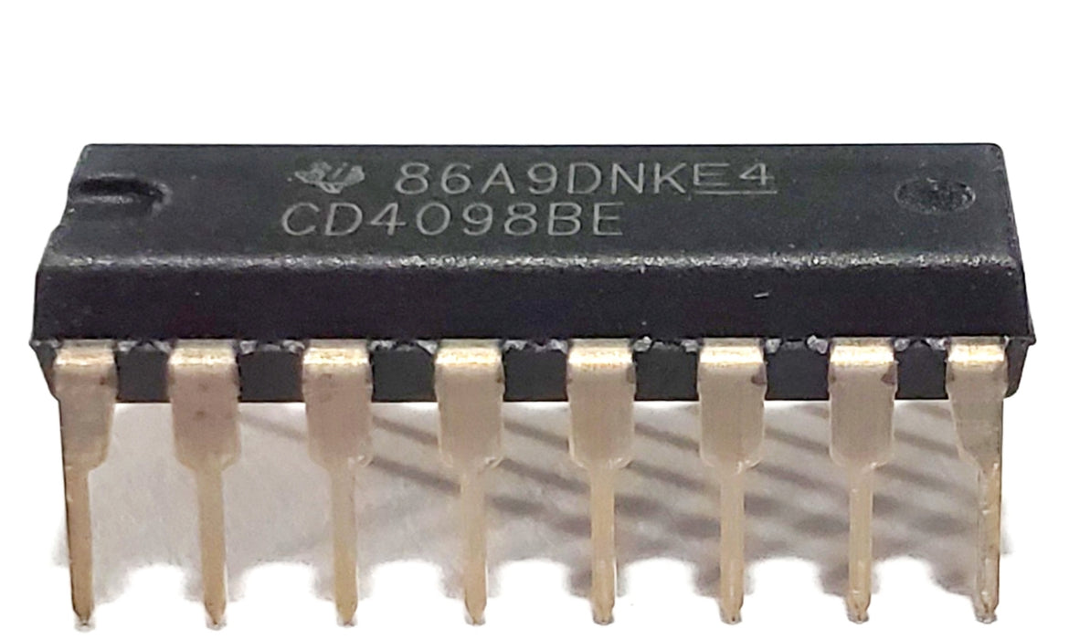
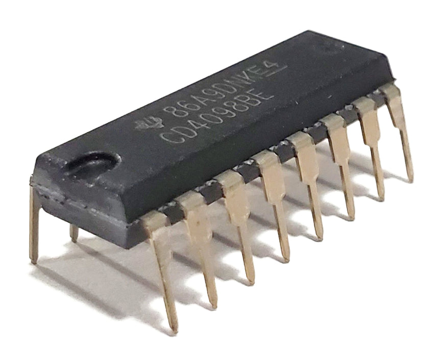
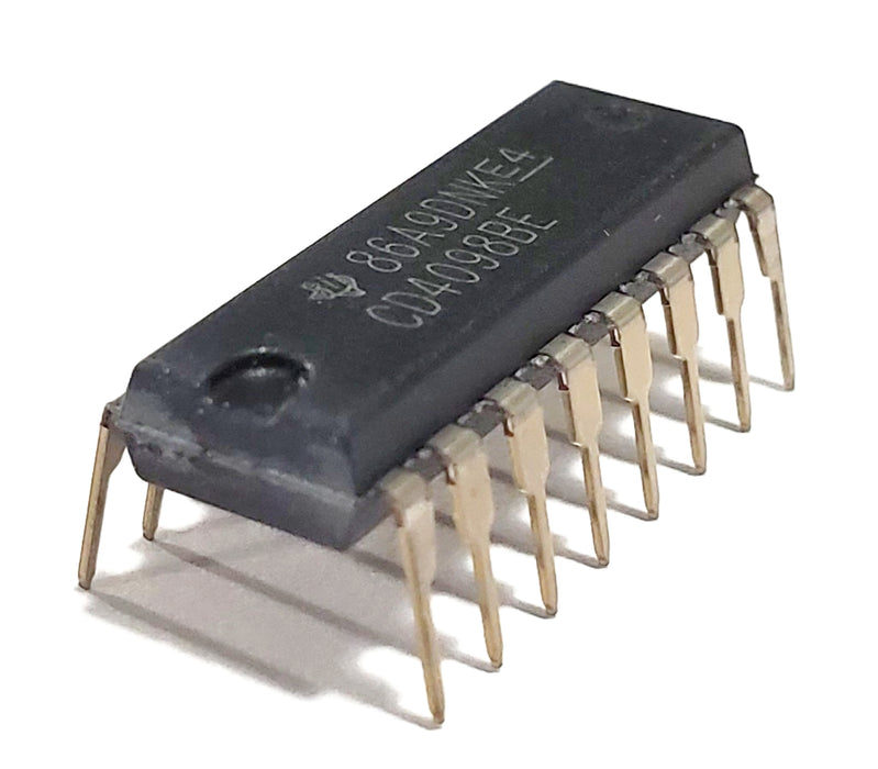
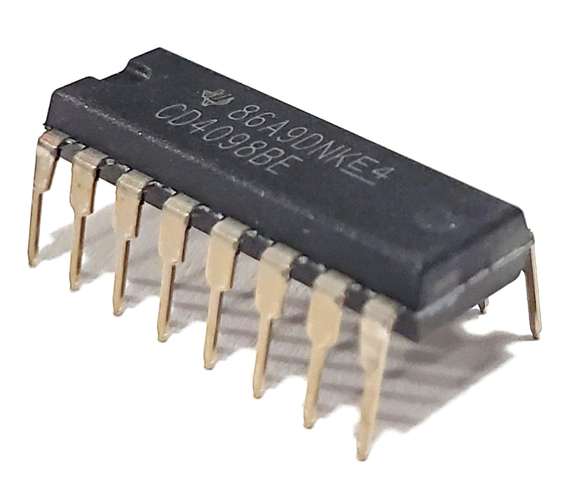
CD4098BE
This item features:
- Retriggerable/resettable capability
- Trigger and reset propagation delays independent of RX, CX
- Triggering from leading or trailing edge
- Q and Q\ buffered outputs available
- Separate resets
- Wide range of output-pulse widths
- 100% tested for maximum quiescent current at 20 V
- Maximum input current of 1 uA at 18 V over full package-temperature range; 100 nA at 18 V and 25°C
- Noise margin (full package-temperature range): 1 V at VDD = 5 V2 V at VDD = 10 V2.5 V at VDD = 15 V5-V, 10-V, and 15-V parametric ratings
- Standardized, symmetrical output characteristics
- Meets all requirements of JEDEC Tentative Standard No. 13B, "Standard Specifications for Description of 'B' Series CMOS Devices."
Applications:
- Pulse delay and timing
- Pulse shaping
- Astable multivibrator
Condition:
- New and Authentic Component(s) - CD4098BE CMOS Dual Monostable Multivibrator ICs.
- Friendly Note: Be mindful of the many, inexpensive, counterfeits available on the market.
General details:
- We are expanding on a daily basis. If you do not see the part, or quantity of the part, you are looking for, please, let us know. We will do our best to accommodate you.